Upravit stránku

Express production of samples fitted with PCB

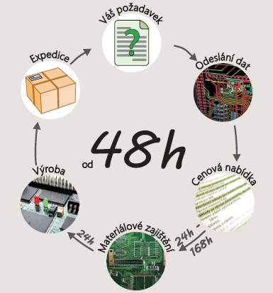
Your agreed price offer till 12:00 pm will be processed by submitting the production of samples fitted with PCB the same day.
The stated times of production of samples fitted with PCB are valid only on Monday - Friday working days.

Production conditions of PCB samples
Maximum number of boards: 3 pieces (up to a maximum area of 4 dm2)

PCB parameters:
number of layers: maximum 6
solder mask
print: 1-2x
surface treatment: chemical gold
material: FR-4
minimum joint thickness: 120 µm
minimum insulation gap thickness: 120 µm
minimum annulus thickness: 120 µm
Minimum bore: 0.25 mm

Data:
PCB gerber RS274-X data Pads, Altium
component list: Excel (Farnell reference)
assembly drawing: pdf
listing component coordinates with reference and rotation angle
  • Fields marked with an asterisk (*) are required.

This website uses cookies

This website is using cookies to provide services, personalize ads, and monitor traffic. By continuing to use this site you are agreeing with usage of cookies. More information.